huawei circuit diagram
Nokia 1100 Full PCB Diagram Mother Board Layout.. 17 Pictures about Nokia 1100 Full PCB Diagram Mother Board Layout. : HUAWEI ALL Model Schematics Diagrams ~ Gtech Mobiles | Huawei, Diagram, HUAWEI p7 phone repair schematic and PCB diagram System update ASCEND and also Nokia C1-00 Full PCB Diagram Mother Board Layout..
Nokia 1100 Full PCB Diagram Mother Board Layout.
 www.u2ugsm.com
1100 nokia diagram pcb mother layout resolution u2ugsm
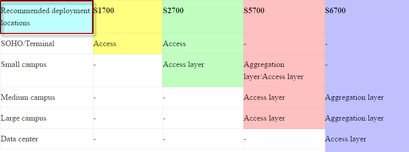
Huawei Fixed Switches Overview – Router Switch Blog
 blog.router-switch.com
switches fixed huawei switch overview locations campus router network enterprise
Huawei Ethernet Switches — Huawei Products
 e.huawei.com
huawei switches data center switch networking ethernet network
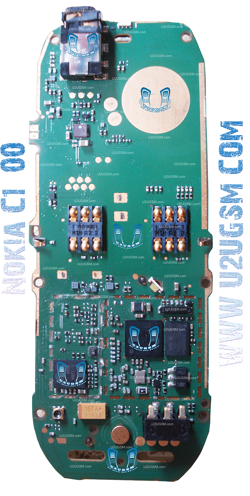
Nokia C1-00 Full PCB Diagram Mother Board Layout.
 www.u2ugsm.com
diagram nokia c1 pcb layout mother motherboard phone cell mobile repairing samsung resolution missing
Nokia 2310 Layout Diagram Of Whole Board
 www.u2ugsm.com
nokia diagram 1600 2310 layout whole 1112 1110i manual lay mobile repair pcb repairing solution service tracing tracks tricks links
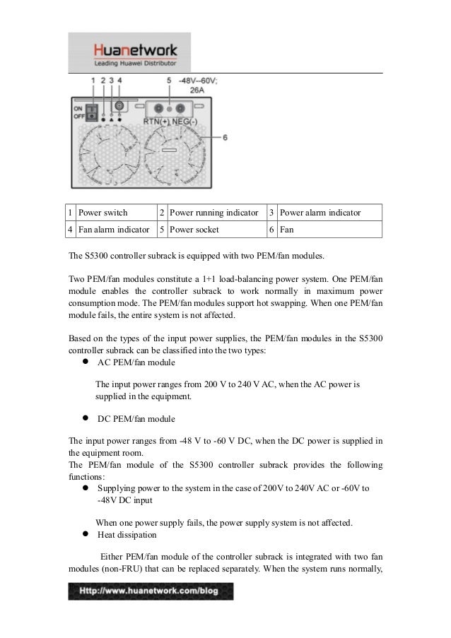
What Is Huawei Quidway S5300 Gigabit Switches
 www.slideshare.net
s5300 quidway
Huawei Y5 II Charging Solution Jumper Problem Ways
 www.u2ugsm.com
huawei y5 ii charging ways solution problem jumper cun u29 battery mobile repair power u2ugsm lite diagram solutions iphone working
HUAWEI P7 Phone Repair Schematic And PCB Diagram System Update ASCEND
 www.aliexpress.com
diagram huawei phone pcb schematic repair manual smartphone g7 lte ascend p7 maintenance reference training smart update system
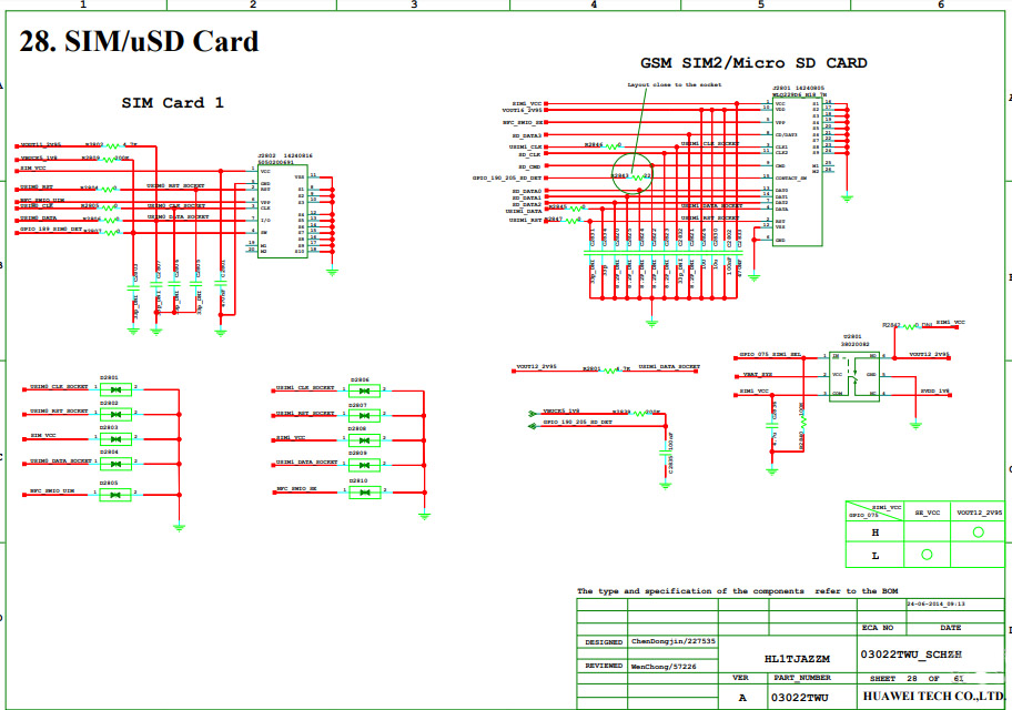
[View 38+] Huawei Schematic Diagram Download
![[View 38+] Huawei Schematic Diagram Download](https://download.huawei.com/mdl/image/download?uuid=849d784ef1294abcb831e480ea886b5e) loughlin-817.blogspot.com
loughlin-817.blogspot.com
megafon russia loughlin
Huawei Honor 10 Lite Charging Solution Jumper Problem Ways | Smartphone
 www.pinterest.com
u2ugsm
Huawei Nova 3i INE LX2 BackLight Ways And Touchscreen Jumper Solution
 www.pinterest.com
3i ine backlight lx2 touchscreen y9 pinout jumpers mobilerdx isp
Huawei Hardware Diagram စုစည္ းမွဴ ~ နည္းပညာ ကိုႏိုင္၀င္း
 konaingwn.blogspot.com
Huawei Y6 Pro Charging Solution Jumper Problem Ways | Phone Solutions
 www.pinterest.com
huawei y6 charging ways solution pro problem jumper diagram mobile power wifi solutions lcd phone 5c repair iphone check laptop
Update Huawei Diagram Pdf ေလး ေတြပါ - H.A.K Mobile Services
 www.hakmobile.top
Huawei Ascend Mate 7 Schematics
 phonelumi.com
schematics
[Download 33+] Huawei P8 Lite Schematic Diagram
![[Download 33+] Huawei P8 Lite Schematic Diagram](https://lh5.googleusercontent.com/proxy/tU7CMCS2YxT_OLw369_FQ5itDpifAScYox1b2CXtNRa9TofDO8S33rXlxOGI6hpNEuBBbSscwfJBqJDG-EKy1ECxu5wffzo6YdhbUMiMR_y2QX8Dr83pYjBfCU12cuqk5UWhb2oEd5j6=s0-d) anten903.blogspot.com
anten903.blogspot.com
teardown
HUAWEI ALL Model Schematics Diagrams ~ Gtech Mobiles | Huawei, Diagram
 www.pinterest.com.mx
huawei diagram
What is huawei quidway s5300 gigabit switches. Diagram nokia c1 pcb layout mother motherboard phone cell mobile repairing samsung resolution missing. Huawei ascend mate 7 schematics